Linear layouts, triton, and linear algebra over F_2
@typedfemale posted the paper “Linear Layouts: Robust Code Generation of Efficient Tensor Computation Using F2” on X (link to tweet). It looked interesting. I tweeted:
“I will actually read this. it’s always the very interesting things that use lin alg over finite fields. i remember in undergrad when i first saw a “real” application of it while learning the general number field sieve.”
I struggled with this paper. This post is the result of that effort. Hopefully, it is useful.
My goal here is to just give a sense of their main idea: using linear algebra over the finite field $F_2$ to manage how tensor data is arranged for computation on GPUs. This is outside my usual area of optimization and machine learning, but anyway it looked like a fun read.
1. GPU and Tensor Layouts
Deep learning models use many tensor computations. GPUs accelerate these computations. The specific arrangement of tensor data on the GPU is called a “tensor layout.” This layout dictates, for example, which register within a specific thread (itself part of a GPU warp, a group of threads executing in lockstep) holds which piece of tensor data for an operation. This layout directly affects performance.
Current methods for defining and managing tensor layouts can apparently be complex.1 They can be specific to particular hardware or operations. This makes it difficult to build systems that are both flexible for different models and hardware, and also consistently fast and error-free. Incorrect or inefficient layouts lead to slow memory access, underused compute units, and slower models.
Triton is a language and compiler, originally developed by OpenAI, for writing custom code segments that run on GPUs, known as GPU kernels. People who train like to write performant ML code use Triton to create these kernels, for example, to fuse multiple operations (like a matrix multiplication followed by an activation function) into a single GPU kernel. The “Linear Layouts” paper aims to improve how Triton’s compiler system handles these tensor layouts.
2. Linear Layouts via Linear Algebra over $\mathbb{F}_2$
The paper “Linear Layouts: Robust Code Generation of Efficient Tensor Computation Using $\mathbb{F}_2$” defines a tensor layout using linear algebra over the finite field $\mathbb{F}_2 = \{0, 1\}$. Each layout is a matrix $A$ with entries in $\mathbb{F}_2$. This matrix $A$ specifies a linear map.
For a distributed layout, this map assigns tensor data to specific hardware processing units and their local storage. The matrix $A$ maps an identifier for a hardware resource to the coordinates of a logical tensor element.
- The input to this map (the domain) is a vector $v \in \mathbb{F}_2^n$. The bits of $v$ identify a unique hardware slot. This vector is a concatenation of bit vectors representing, for example, a register index $v_{\text{reg}}$, a thread index $v_{\text{thr}}$, and a warp index $v_{\text{wrp}}$, so $v = [v_{\text{reg}} | v_{\text{thr}} | v_{\text{wrp}}]$.
- The output of the map (the codomain) is a vector $w \in \mathbb{F}_2^m$. The bits of $w$ are the binary representation of the coordinates of an element in the logical tensor. For a 2D tensor
Tensor[i,j], $w$ would be formed by concatenating the binary representations of the integer indices $i$ and $j$, e.g., $w = [\text{bits}(i) | \text{bits}(j)]$. - The mapping is $w = Av$. All matrix and vector operations use $\mathbb{F}_2$ arithmetic, where addition is XOR and multiplication is AND.
This matrix $A$ dictates which hardware slot $v$ is responsible for which logical tensor element $w$. The authors state this system can represent existing layouts, such as those in Triton, and define new ones because these mappings from hardware bit identifiers to logical coordinate bit identifiers can be expressed as such matrices.
Example: Layout A from Figure 1 (Page 4 of the Paper)
Figure 1a in the paper illustrates two distributed layouts.
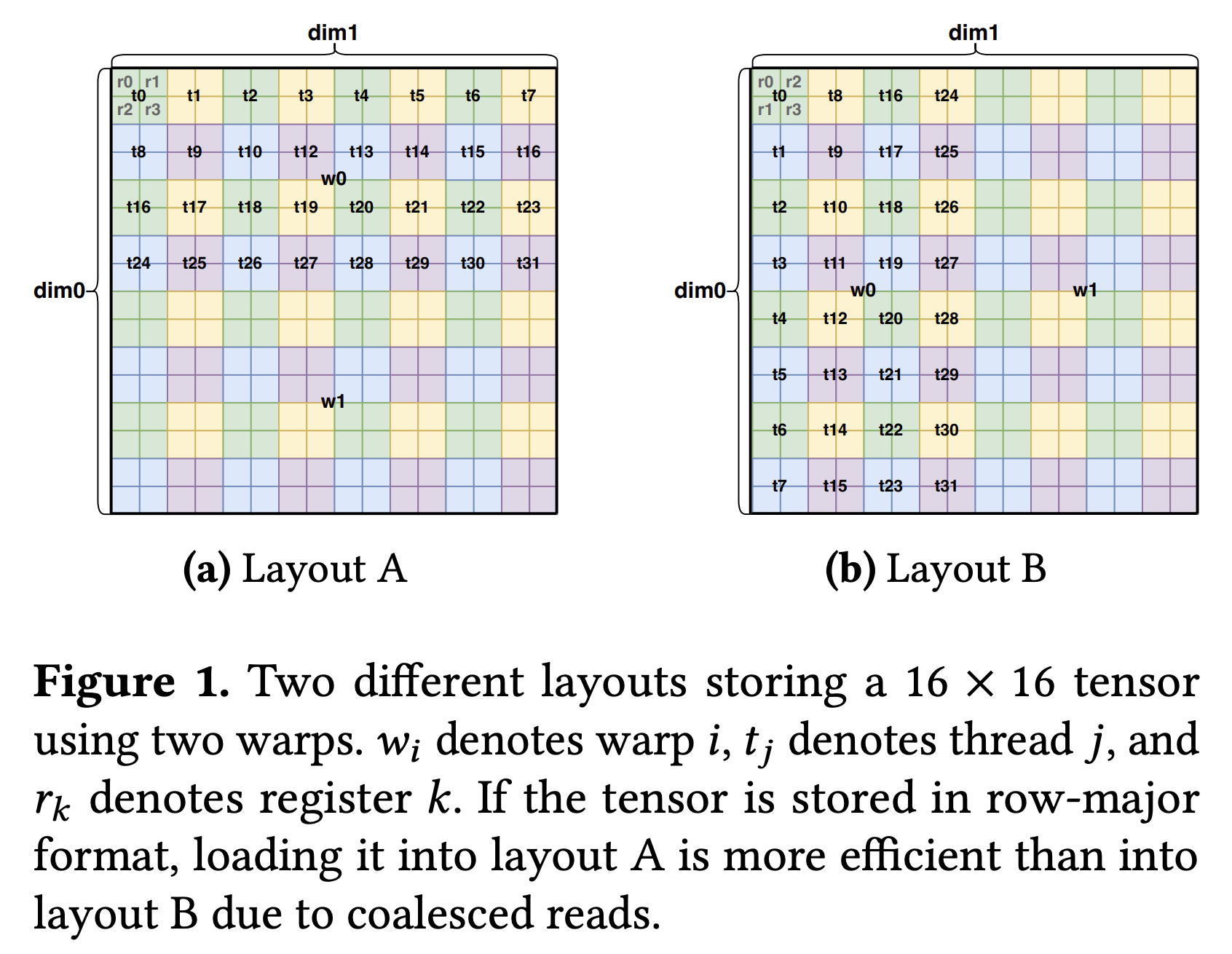
Let’s look into Layout A, which can be represented by a $8 \times 8$ matrix $A$ with entries in $\mathbb{F}_2$. This matrix maps an 8-bit hardware ID $v$ to an 8-bit logical coordinate $w$ for a $16 \times 16$ tensor.
-
Input:
\[v = [v_0(\text{reg}_0) \, v_1(\text{reg}_1) \,|\, v_2(\text{thr}_0) \, v_3(\text{thr}_1) \, v_4(\text{thr}_2) \, v_5(\text{thr}_3) \, v_6(\text{thr}_4) \,|\, v_7(\text{wrp}_0)]^T\](Bit $v_k$ is the $k$-th component of $v$; labels like $\text{reg}_0$ indicate conceptual roles).
-
Output:
\[w = [w_0(i_0) \, w_1(i_1) \, w_2(i_2) \, w_3(i_3)\, |\, w_4(j_0) \, w_5(j_1) \, w_6(j_2) \, w_7(j_3) ]^T\]The bits $w_0..w_3$ form the column index $j$ ($j_0$ is LSB). The bits $w_4..w_7$ form the row index $i$ ($i_0$ is LSB).
Note we’re slightly deviating from the paper. There, they define $w_{0:3} = j$ and $w_{4:7} = i$. I find it more natural to define $w_{0:3} = i$ and $w_{4:7} = j$. This means that $j = w_7\cdot 2^3 + w_6 \cdot 2^2 + w_5\cdot 2^1 + w_4\cdot 2^0$, etc
To construct the matrix $A$ frin Figure 1a for this linear layout, we observe that it’s mapping $w = Av$ has the following effect.
- Incrementing $v_0$ (respectively, $v_1$) increments $j$ by $1$ (respectively, $i$ by $1$). Thus, the least significant bit $w_4$ of $j$ (respectively $w_0$ of $i$) is precisely $v_0$ (respectively $v_1$).
- Incrementing $v_2$ increments $j$ by $2$. Thus, the second bit $w_5$ of $j$ is precisely $v_2$. Likewise, incrementing $v_5$ by $1$ increments $i$ by $2$, so the second bit $w_2$ of $i$ is precisely $v_5$.
Continuing with similar reasoning, we can show the following:
\[A = \begin{pmatrix} % v0 v1 v2 v3 v4 v5 v6 v7 0 & 1 & 0 & 0 & 0 & 0 & 0 & 0 \\ % w0 (i0) 0 & 0 & 0 & 0 & 0 & 1 & 0 & 0 \\ % w1 (i1) 0 & 0 & 0 & 0 & 0 & 0 & 1 & 0 \\ % w2 (i2) 0 & 0 & 0 & 0 & 0 & 0 & 0 & 1 \\ % w3 (i3) 1 & 0 & 0 & 0 & 0 & 0 & 0 & 0 \\ % w4 (j0) 0 & 0 & 1 & 0 & 0 & 0 & 0 & 0 \\ % w5 (j1) 0 & 0 & 0 & 1 & 0 & 0 & 0 & 0 \\ % w6 (j2) 0 & 0 & 0 & 0 & 1 & 0 & 0 & 0 % w7 (j3) \end{pmatrix}\]From this matrix, you can verify that it indeed maps various hardware ids slots to the correct logical tensor elements. For example, the slot with the slot corresponding to register 0, thread 0, warp 0 maps to the logical tensor element Tensor[0,0], $i = w_{3:0} = 0000$ and $j = w_{7:4} = 0000$ (notice I reversed the bits). On other hand, the slot corresponding to register 1, thread 1, warp 0 maps to the logical tensor element Tensor[0,3], $i = w_{3:0} = 0000$ and $j = w_{7:4} = 0011$.
3. Memory Layouts and Shared Memory Interaction
Distributed layouts assign tensor elements to hardware compute units. Memory layouts describe how these logical tensor elements are arranged linearly within a memory segment, such as a GPU’s global or shared memory. A memory layout can be represented by a matrix $M_{\text{mem}}$ with entries in $\mathbb{F}_2$. This matrix $M_{\text{mem}}$ maps a vector representing a memory offset to the bits of the logical tensor coordinate stored at that offset:
logical_tensor_coordinate = M_mem * memory_offset_bits.
When we know the logical coordinate of a tensor element and need to find its location in memory, we use the inverse map, $M_{\text{mem_inv}}$. This matrix maps the bits of a logical tensor coordinate to the bits of its memory offset:
memory_offset_bits = M_mem_inv * logical_tensor_coordinate_bits.
A Simple Memory Layout: Row-Major Order
To understand memory access patterns, we first consider a basic row-major arrangement for a $16 \times 16$ tensor, Tensor[i,j]. The linear memory offset is offset = i * 16 + j (assuming unit-sized elements). Suppose the logical coordinate vector $w$ follows our convention: $w = [w_0(i_0) \dots w_3(i_3) | w_4(j_0) \dots w_7(j_3)]^T$. Here, $w_{0..3}$ are the bits of $i$ (LSB $i_0$ to MSB $i_3$), and $w_{4..7}$ are the bits of $j$ (LSB $j_0$ to MSB $j_3$). The memory offset $k$ is an 8-bit value $k = [k_0(\text{MSB}) \dots k_7(\text{LSB})]^T$. For row-major storage, the column index $j$ forms the lower-order bits of the offset ($k_{0..3}$), and the row index $i$ forms the higher-order bits ($k_{4..7}$).
The matrix $M_{\text{mem_inv}}: w \mapsto k$ that achieves this is an $8 \times 8$ permutation matrix:
This matrix $M_{\text{mem_inv}}$ takes $w=[\text{bits}(i) | \text{bits}(j)]$ and produces $k=[\text{bits}(j) | \text{bits}(i)]$, correctly placing $j$-bits into the lower part of $k$ and $i$-bits into the higher part.
GPU Shared Memory Structure
A GPU’s shared memory is a fast, on-chip memory. It is physically divided into multiple (e.g., 32) independent banks. Each bank contains many addressable lines (also called vector words or cache lines), typically the size of a wide hardware memory access (e.g., 128 bits). Each line stores multiple individual data elements (e.g., four 32-bit floats).
A specific data element within shared memory is pinpointed by three components:
bank_hw: Selects the physical bank.idx_hw: Selects the line (vector word) within that bank.vec_hw: Selects the specific element within that chosen line.
A useful way to visualize this memory is:
bank 0: [line 0, line 1, line 2, ..., line N-1]
bank 1: [line 0, line 1, line 2, ..., line N-1]
...
bank 31: [line 0, line 1, line 2, ..., line N-1]
Accessing different banks simultaneously is done in parallel (to my knowledge). Accessing the same bank simultaneously by different threads for different lines causes bank conflicts, serializing operations. On the other hand, accessing elements within the same line simultaneously can be performed in parallel; this is called vectorized access. Efficient memory access thus requires careful mapping of data to these (vec_hw, bank_hw, idx_hw) components.
The Swizzling Map s
The paper’s “optimal swizzling” algorithm constructs a specialized memory layout for shared memory, defined by an $\mathbb{F}_2$ matrix $s$. This map $s$ defines how the structured shared memory hardware components map to the logical tensor coordinate stored at that physical slot:
- Input (domain): A bit vector
v_sm = [vec_hw | idx_hw | bank_hw]representing a shared memory slot description. - Output (codomain): The logical tensor coordinate $w = [\text{bits}(i) | \text{bits}(j)]$ (using our convention for $w$) stored at that slot.
- Mapping: $w = s \cdot v_{\text{sm}}$.
The purpose of constructing this swizzling map $s$ is to arrange logical data across physical shared memory slots in a non-obvious (“swizzled”) manner. This design ensures that when threads (operating under a given distributed layout) need to access various logical tensor coordinates, the corresponding shared memory hardware slots (vec_hw, idx_hw, bank_hw) (found via $s^{-1}(w)$) are distributed to minimize bank conflicts and enable efficient vectorized reads and writes.
4. Linear Algebra and Layouts
A compiler must perform several tasks to generate efficient GPU code: it must arrange data for memory access, rearrange it for computation, and map these operations to specialized hardware instructions. Representing layouts as matrices allows the compiler to perform these tasks using linear algebra.
Layout Conversion Between Layouts Optimized for Memory and Compute
We can use matrix products to represent how a GPU kernel moves data between a layout optimized for memory access and one required by a compute unit.
Loading data from global memory is fastest when threads access contiguous blocks of memory, a pattern known as coalesced access. This suggests a simple, row-major layout. However, a specialized compute unit, like a Tensor Core, may require data to be presented in a completely different layout to perform its calculations. We can compute this conversion using matrix products.
Let layout $A$ be the source (e.g., memory layout) and $B$ be the destination (e.g., compute layout). We need to find the transformation $C$ that maps a hardware resource $v_A$ in the source layout to its corresponding resource $v_B$ in the destination. The same logical data $w$ must satisfy $w = Av_A$ and $w = Bv_B$.
For layout $B$ to be a valid destination, it must be surjective, i.e., its mapping can reach every element of the logical tensor. This guarantees that a right inverse $B^{-1}$ exists. By setting the expressions for $w$ equal, we find the conversion map:
\[v_B = (B^{-1}A)v_A\]The structure of the resulting matrix $C = B^{-1}A$ describes the hardware operations needed to move data. For example, if $C$ only permutes register bits, the conversion is a simple move between registers within each thread. If it mixes bits between different threads within a warp, it requires an “intra-warp shuffle,” a hardware instruction that exchanges data between threads in the same execution group.
Product Operator for Hierarchical Layout Design
The product operator constructs complex layouts from simpler component layouts. This process corresponds to creating a block-diagonal matrix. A developer can define a layout for registers within a thread ($L_{reg}$) and a layout for the threads in a warp ($L_{thr}$) separately. The product operator $L_{reg} \times L_{thr}$ combines them into a single layout $L$ for the entire warp. The matrix for $L$ is the block-diagonal composition of its component matrices:
\[L = \begin{pmatrix} L_{reg} & 0 \\ 0 & L_{thr} \end{pmatrix}\]Left Division for Matching Hardware Instructions
Left division determines if a data layout can be loaded or stored using a specialized hardware instruction. An instruction like ldmatrix loads a fixed-size tile of data from shared memory into registers. Its operation is defined by a corresponding tile layout, a small matrix $T$. This matrix maps the hardware resources for a single instruction call (e.g., the bits of the register IDs) to the data it acts upon (e.g., the bits of the memory offsets).
The compiler checks if the kernel’s larger data layout $L$ is compatible with the instruction’s tile layout $T$. This is not arithmetic division. It is a test of matrix structure. Left division $L / T$ succeeds if $L$ can be decomposed into the block-diagonal form:
\[L = \begin{pmatrix} T & 0 \\ 0 & R \end{pmatrix}\]where $R$ is the remainder layout. This decomposition confirms that a subset of $L$’s input resources maps to a subset of its output data using a transformation that is structurally identical to $T$, with no interference from the other resources governed by $R$.
If the division succeeds, the compiler can generate a sequence of ldmatrix instructions to load the data for the entire layout $L$. The tile layout $T$ governs the loading of the first block. The remainder layout $R$ is then used to calculate the starting address for the next block, and the process is repeated. This automates the use of high-throughput hardware instructions for any compatible layout.
Unification of Triton’s Layouts
In Triton’s legacy system, conversions between different layout types led to a “quadratic explosion” of custom implementations. Each pair of layouts required a unique, manually-coded conversion function. This made the compiler complex and difficult to extend, as adding a new layout type required implementing new conversion paths to all existing types.
The paper proves that all of Triton’s legacy layouts can be represented as linear layouts (Theorem 4.9). This result allows the compiler to replace the entire system of custom conversion functions with a single matrix operation. The conversion from any layout $A$ to any layout $B$ is now specified by the matrix product $B^{-1} A$.
This simplifies compiler development. To add a new layout, a developer provides its matrix definition. Conversions to and from all other defined layouts are then handled by the existing matrix product operation.
5. Optimizing Code
The framework allows a compiler to automate optimizations by translating them into questions about matrix properties.
Vectorization
Previously, Triton identified vectorization opportunities by finding a tensor’s fastest-running dimension and assuming it determined contiguity. This heuristic fails for a tensor of shape [128, 1]. The fastest-running dimension has size 1, so Triton would disable vectorization, even though 128 contiguous elements are available along the other dimension.
The linear layout method replaces this inference with a direct computation. The physical property of contiguous logical elements being stored in contiguous registers is equivalent to an identity map on their address bits.
More specifically, the compiler queries the layout’s inverse matrix, $L^{-1}$. It finds the largest integer $k$ for which the $k \times k$ sub-matrix mapping the lowest-order logical bits to the lowest-order register bits is the identity matrix. This $k$ is the precise vectorization width, calculated directly from the layout’s structure.
Broadcasting
Broadcasting is the replication of a single logical element across multiple hardware resources, such as different threads. In a reduction operation, like a sum, these duplicated values must be counted only once to avoid incorrect results.
Linear layouts provide a direct method for identifying this replication. Specifically, the duplication of a logical element across threads is represented in the layout matrix $A$ as a zero-column in the section corresponding to the thread ID bits.
A zero-column means that changing the thread ID does not change the resulting logical address $w$ in the mapping $w = Av$. The compiler inspects the matrix for this property to ensure each logical element is processed only once during a reduction.
Mixed-Precision Data Shuffling
A mixed-precision matrix multiplication computes the product of two matrices with different data types, such as mxfp4 and bf16. The overall computation is tiled, meaning it is broken down into smaller matrix multiplications on tiles of the input data. A performance bottleneck arises if the bf16 tiles cannot be loaded into registers as efficiently as the mxfp4 tiles.
The GPU hardware can execute wide vector instructions, which load a fixed-size block of data (e.g., 16 bytes) from a contiguous block of memory addresses in a single operation. The challenge is to arrange the data in memory such that all elements needed for a single compute tile are physically contiguous and can be fetched with one of these instructions.
For the bf16 data type, a standard memory layout may not have this property. The solution is a data shuffle: a pre-processing step that copies the bf16 data into a new arrangement within on-chip shared memory, organizing it so that each tile’s worth of data resides in a contiguous block of addresses.
The user specifies the logic of this shuffle with a high-level shape operation. For instance, if the hardware instruction expects a tile’s data in a layout that is logically the transpose of what a simple load provides, the user specifies a tt.transpose operation.
This shape operation is a linear transformation on the tensor’s logical coordinates and is represented by a permutation matrix, $T_{shape}$. The compiler combines this with the original layout matrix, $A_{bf16}$, to compute the new, shuffled layout $A_{shuffled}$:
\[A_{shuffled} = T_{shape}A_{bf16}\]The compiler uses this resulting matrix $A_{shuffled}$ to generate the code that performs the physical memory copy for the shuffle.
Generating Code for Layout Conversions
To convert a tensor from a source distributed layout $A$ to a destination distributed layout $B$, the compiler first computes the conversion matrix $C = B^{-1}A$. This matrix maps the source hardware resources to the destination hardware resources. The structure of $C$ determines the cheapest hardware primitive that can perform the conversion.
The compiler checks the structure of $C$ in order of cost, from cheapest to most expensive.
-
Intra-thread Register Move: This is the cheapest conversion. It is possible if the data movement is confined entirely within each thread. This is the case if the conversion matrix $C$ only permutes register bits, meaning the sub-matrix $(B^{-1}A)_{reg}$ is a permutation matrix and the rest of $C$ is the identity.
-
Intra-warp Shuffle: If an intra-thread move is not possible, the compiler checks if the conversion can be done with warp shuffles. A warp shuffle is a hardware instruction that allows threads within the same warp to exchange data directly without using shared memory. This is possible if the conversion matrix $C$ does not move data between warps, which corresponds to the warp-related block of the matrix, $(B^{-1}A)_{wrp}$, being the identity matrix.
-
Inter-warp Conversion via Shared Memory: If neither of the above conditions is met, data must move between different warps. This is the most expensive conversion and requires using on-chip shared memory as an intermediary. Data from the source warps is written to shared memory and then read by the destination warps.
Generating Warp Shuffles
When a conversion requires an intra-warp data exchange, the compiler generates a sequence of hardware shfl.sync instructions. A receiving thread executes shfl.sync(value, srcLane) to fetch a value from the registers of a sending thread, identified by its lane index srcLane. The linear layout framework provides a direct method for calculating these parameters.
This process is illustrated by the example in Figure 3.
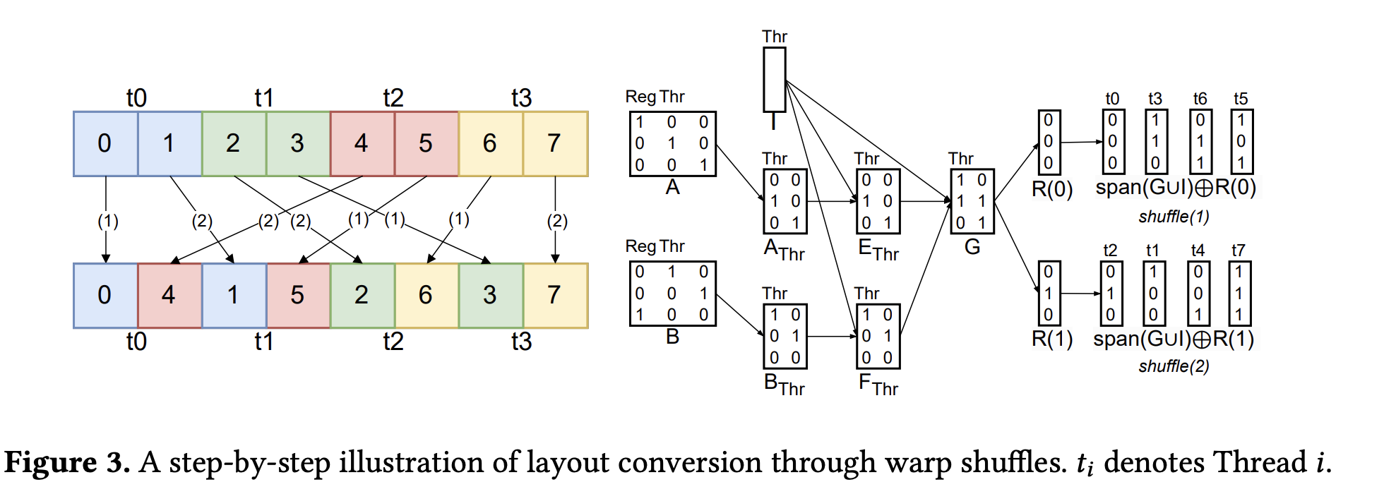 Figure 3: Layout conversion via warp shuffles from the paper. The labels
 t_i denote 3-bit logical address vectors. Note that the t0,..,t7 in the top right corner are not threads, they are just labels for the basis vectors.
1. Determine the Exchange Vector ($V$)
First, the compiler identifies data that can be moved as a single vector. This data corresponds to the intersection of the register-related column subspaces, $A_{reg} \cap B_{reg}$. Any data in this subspace maintains its relative position within the registers during the conversion.
Because this block of data is structurally invariant, it can be moved as a single unit. The compiler selects a basis $V$ for the largest possible subspace within this intersection whose total data size does not exceed the hardware’s 32-bit shfl.sync payload limit. This basis $V$ defines the vector that will be moved in each shuffle instruction.
2. Decompose the Address Space
The compiler creates a plan by decomposing the logical address space, which combines register and thread addresses. It computes bases for several subspaces.
- $I = \text{span}(A_{thr}) \cap \text{span}(B_{thr})$: Data that does not move between threads.
- $E = A_{thr} \setminus I$ and $F = B_{thr} \setminus I$: Subspaces of data to be sent and received.
- $G = {e_i \oplus f_i}$: The set of displacement vectors. The paper specifies that $G$ is constructed “After choosing an ordering for $E$ and $F$.” This implies a one-to-one pairing $(e_i, f_i)$ based on the chosen ordering of the basis vectors. This pairing is necessary because the conversion is a permutation: each source data element $e_i$ has a unique destination $f_i$.
- $R$: A basis for the intra-thread (register) address space. This is a basis for the complement of the thread space not already covered by the vectorized subspace $V$, $\text{span}(A_{thr} \cup B_{thr} \cup V)$.
3. Sequence the Exchange
A thread holds more data than one shuffle can move. The exchange is thus partitioned into rounds, one for each basis vector in $R$. A larger vectorization $V$ results in a smaller basis $R$ and fewer rounds.
In Figure 3, $V$ is empty, $R$ has two vectors, $R(0)$ and $R(1)$, corresponding to the two data elements held by each thread.
- Round 1 (
shuffle(1)): This round moves the data slice whose logical addresses are in the affine subspace $\text{span}(G \cup I) \oplus R(0)$. A single data element’s logical address is $e_i \oplus R(0)$.valueparameter: Thevalueis the vector defined by $V$ from the register slice selected by $R(0)$.srcLaneparameter: A receiving thread at a destination thread address $f_i$ uses its corresponding displacement $g_i$ to find its source thread address $e_i = f_i \oplus g_i$. The integer representation of this vector $e_i$ is used as thesrcLane.
- Round 2 (
shuffle(2)): This round moves the data slice corresponding to the second register, selected by $R(1)$. The logical addresses are $\text{span}(G \cup I) \oplus R(1)$. Thevalueis now the data from the second register slice, but thesrcLanefor each thread is calculated using the same exchange pattern $G$ as in the first round.
Running Out of Steam
There is a bunch of other cool stuff in the paper. I ideally wanted to present “optimal swizzling,” but I timeboxed this post, and so I think I’ll end it here.
-
From what I can understand. I am not a GPU expert, but I will write like I am one for the purpose of this post. ↩